SFP+-10G-850nm-300m-MM-LC
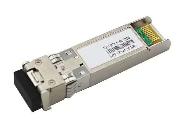
SFP+-10G-1310nm-10KM-SM-LC
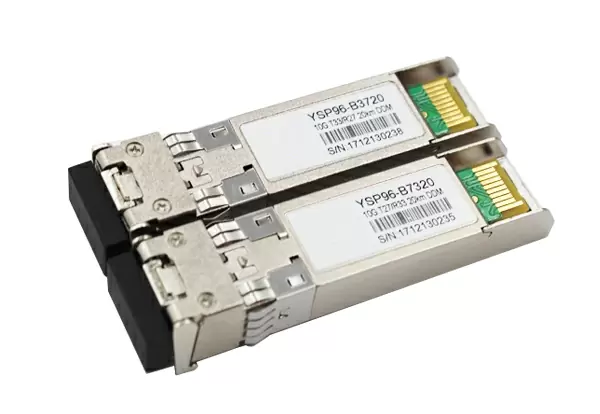
SFP+-10G-1310nm-20KM-SM-LC
SFP+-10G-1550nm-40KM-SM-LC
SFP+-10G-1550nm-80KM-SM-LC
Features
ü Up to 10.6Gbps data links
ü 1310nm DFB Laser and PIN photo-detector
ü Up to 20km on 9/125µm SMF
ü Duplex LC receptacle optical interface compliant
ü Hot pluggable
ü All-metal housing for superior EMI performance
ü RoHS6 compliant (lead free)
ü Operating case temperature:
Commercial: -5ºC to +70°C
Extended: -20ºC to +80°C
Industrial: -40ºC to +85°C
Applications
ü 10GBASE-LR/LW 10G Ethernet
ü 10G Fibre Channel
ü 10G SONET
ü Other optical links
Standards
ü Compliant with SFP+ MSA
ü Compliant with SFF-8472
ü Compatible with IEEE802.3ae
Description
The SFP+ transceivers are designed for use in 10-Gigabit Ethernet links up to 20km over Single Mode Fiber.
The transceivers are compatible with SFP+ MSA and SFF-8472. For further information, please refer to SFP+ MSA and SFF-8472.
Module Block Diagram

Absolute Maximum Ratings
Parameter | Symbol | Min. | Typical | Max. | Unit |
Power Supply Voltage | VCC | 0 |
| 3.6 | V |
Storage Temperature | Ts | -40 |
| +85 | °C |
Relative Humidity | RH | 0 |
| 85 | % |
RX Input Average Power | Pmax | - |
| 1.5 | dBm |
Recommended Operating Environment
Parameter | Symbol | Min. | Typical | Max. | Unit |
Power Supply Voltage | VCC | 3.13 | 3.3 | 3.46 | V |
Power Supply Current | ICC |
|
| 300 | mA |
Operating Case Temperature | Commercial | TC | -5 |
| +70 | °C |
Extended | -20 |
| +80 |
Industrial | -40 |
| +85 |
Data Rate |
|
| 10.3125 |
| Gbps |
Electrical Characteristics
Parameter | Symbol | Min. | Typical | Max. | Unit | Note |
Transmitter Section |
|
Input Differential Impedance | Rin | 90 | 100 | 110 | Ω |
|
Differential Data Input Swing | Vin PP | 180 |
| 700 | mV | 1 |
Transmit Disable Voltage | VD | Vcc – 1.3 |
| Vcc | V |
|
Transmit Enable Voltage | VEN | Vee |
| Vee+ 0.8 | V |
|
Receiver Section |
|
Differential Data Output Swing | Vout PP | 300 |
| 850 | mV |
|
LOS Fault | Vlos fault | Vcc – 0.5 |
| Vcc_host | V | 2 |
LOS Normal | Vlos norm | Vee |
| Vee+0.5 | V | 2 |
Notes:
1. Connected directly to TX data input pins. AC coupling from pins into laser driver IC.
2. LOS is an open collector output. Should be pulled up with 4.7kΩ – 10kΩ on the host board. Normal operation is logic 0; loss of signal is logic 1.
Optical Parameters
Parameter | Symbol | Min. | Typical | Max. | Unit | Note |
Transmitter Section |
Centre Wavelength | λc | 1260 | 1310 | 1355 | nm |
|
Spectral Width(-20dB) | Δλ |
|
| 1 | nm |
|
Side Mode Suppression Ratio | SMSR | 30 |
|
| dB |
|
Average Optical Power (avg.) | Pout | -5.0 |
| +1 | dBm | 1 |
Laser Off Power | Poff | - | - | -30 | dBm |
|
Extinction Ratio | ER | 3.5 | - | - | dB | 2 |
Relative Intensity Noise | RIN | - | - | -128 | dB/Hz |
|
Optical Rise/Fall Time | tr / tf |
| - | 50 | ps | 3 |
Optical Return Loss Tolerance |
| - | - | 12 | dB |
|
Output Optical Eye | Compliant with IEEE802.3ae eye masks when filtered | 2 |
Receiver Section |
|
Receiver Center Wavelength | λc | 1260 |
| 1620 | nm |
|
Receiver Sensitivity in Average Power | Sen | -14.4 |
| 0.5 | dBm | 4 |
Los Assert | LOSA | -30 | - | - | dBm |
|
Los Dessert | LOSD | - | - | -16 | dBm |
|
Los Hysteresis | LOSH | 0.5 | - | 5 | dB |
|
Overload | Pin-max | - | - | 0.5 | dBm | 4 |
Receiver Reflectance |
| - | - | -12 | dB |
|
Receiver power (damage) |
| - | - | 1.5 | dBm |
|
Notes:
1. The optical power is launched into 9/125µm SMF.
2. Measured with a PRBS 231-1 test pattern @10.3125Gbps.
3. Unfiltered, 20-80%. Measured with a PRBS 231-1 test pattern @10.3125Gbps.
4. Measured with a PRBS 231-1 test pattern @10.3125Gbps, ER=4dB, BER <10-12.
Timing Characteristics
Parameter | Symbol | Min. | Typical | Max. | Unit |
TX_Disable Assert Time | t_off |
|
| 100 | us |
TX_Disable Negate Time | t_on |
|
| 2 | ms |
Time to Initialize | t_start_up |
|
| 300 | ms |
Tx_Fault Assert | t_fault_on |
|
| 1 | ms |
Tx_Fault Reset | t_reset | 10 |
|
| us |
Rx_LOS Assert Delay | t_los_on |
|
| 100 | us |
Rx_LOS Negate Delay | t_los_off |
|
| 100 | us |
Clock Frequency | fSCL | 0 |
| 400 | kHz |
Digital Diagnostic Monitor Characteristics (DDM)
The following digital diagnostic characteristics are defined over the Recommended Operating Environment unless otherwise specified. It is compliant to SFF8472 Rev10.2 with internal calibration mode. For external calibration mode please contact our sales stuff.
Parameter | Symbol | Min. | Max. | Unit |
Temperature Monitor Absolute Error | DMI_Temp | -3 | 3 | °C |
Laser Power Monitor Absolute Error | DMI_TX | -3 | 3 | dB |
RX Power Monitor Absolute Error | DMI_RX | -3 | 3 | dB |
Supply Voltage Monitor Absolute Error | DMI_VCC | -3% | 3% | V |
Bias Current Monitor Absolute Error | DMI_Ibias | -10% | 10% | mA |
Digital Diagnostic Memory Map (Compliant with SFF-8472)
The transceivers provide serial ID memory contents and diagnostic information about the present operating conditions by the 2-wire serial interface (SCL, SDA).
The diagnostic information with internal calibration or external calibration all are implemented, including received power monitoring, transmitted power monitoring, bias current monitoring, supply voltage monitoring and temperature monitoring.
The digital diagnostic memory map specific data field defines as following (For further information, please refer to SFF-8472).

Pin Definitions

Pin Descriptions
Pin | Signal Name | Description | Plug Seq. | Notes |
1 | VeeT | Module Transmitter Ground | 1 | 1 |
2 | TX FAULT | Module Transmitter Fault | 3 |
|
3 | TX Disable | Transmitter Disable; Turns off transmitter laser output | 3 |
|
4 | SDA | 2-Wire Serial Interface Data Line | 3 | 2 |
5 | SCL | 2-Wire Serial Interface Clock | 3 | 2 |
6 | Mod_ABS | Module Definition, Grounded in the module | 3 |
|
7 | RS0 | Receiver Rate Select (not used) | 3 |
|
8 | LOS | Receiver Loss of Signal Indication Active LOW | 3 |
|
9 | RS1 | Transmitter Rate Select (not used) | 3 |
|
10 | VeeR | Module Receiver Ground | 1 | 1 |
11 | VeeR | Module Receiver Ground | 1 | 1 |
12 | RD- | Receiver Inverted Data Output | 3 |
|
13 | RD+ | Receiver Non-Inverted Data Output | 3 |
|
14 | VeeR | Module Receiver Ground | 1 | 1 |
15 | VccR | Module Receiver 3.3 V Supply | 2 |
|
16 | VccT | Module Transmitter 3.3 V Supply | 2 |
|
17 | VeeT | Module Transmitter Ground | 1 | 1 |
18 | TD+ | Transmitter Non-Inverted Data Input | 3 |
|
19 | TD- | Transmitter Inverted Data Input | 3 |
|
20 | VeeT | Module Transmitter Ground | 1 | 1 |
Notes:
Plug Seq.: Pin engagement sequence during hot plugging.
1. Module ground pins GND are isolated from the module case.
2. Shall be pulled up with 4.7K-10Kohms to a voltage between 3.15V and 3.45V on the host board.
Recommended Power Interface Circuit

Recommended Interface Circuit

Mechanical Dimensions

Ordering information
Level | Product Description |
Commercial | 850nm, 10Gbps, 300m, Duplex LC SFP+ Transceiver, -5ºC ~ +70ºC, With DDM. |
Industrial | 850nm, 10Gbps, 300m, Duplex LC SFP+ Transceiver, -40ºC ~ +85ºC, With DDM. |
Level | Product Description |
Commercial | 1310nm, 10Gbps, 10km, Duplex LC SFP+ Transceiver, -5ºC ~ +70ºC, With DDM. |
Industrial | 1310nm, 10Gbps, 10km, Duplex LC SFP+ Transceiver, -40ºC ~ +85ºC, With DDM. |
Level | Product Description |
Commercial | 1310nm, 10Gbps, 20km, Duplex LC SFP+ Transceiver, -5ºC ~ +70ºC, With DDM. |
Industrial | 1310nm, 10Gbps, 20km, Duplex LC SFP+ Transceiver, -40ºC ~ +85ºC, With DDM. |
Level | Product Description |
Commercial | 1550nm, 10Gbps, 40km, Duplex LC SFP+ Transceiver, -5ºC ~ +70ºC, With DDM. |
Industrial | 1550nm, 10Gbps, 40km, Duplex LC SFP+ Transceiver, -40ºC ~ +85ºC, With DDM. |
Level | Product Description |
Commercial | 1550nm, 10Gbps, 80km, Duplex LC SFP+ Transceiver, -5ºC ~ +70ºC, With DDM. |
Industrial | 1550nm, 10Gbps, 80km, Duplex LC SFP+ Transceiver, -40ºC ~ +85ºC, With DDM. |