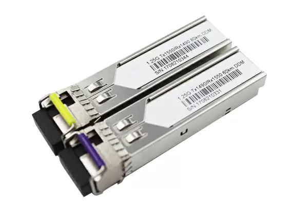
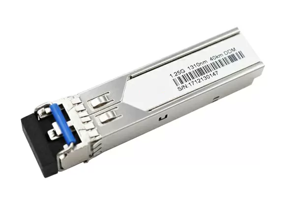
SFP-1.25G-1310nm-2km-MM-LC
Features
ü Up to 1.25Gbps data links
ü 1310nm FP Laser and PIN photo-detector
ü Up to 2km on 50/125µm MMF
ü Duplex LC receptacle optical interface compliant
ü Hot pluggable
ü All-metal housing for superior EMI performance
ü RoHS6 compliant (lead free)
ü Operating case temperature:
Commercial: -5°C to +70°C
Extended: -20°C to +80°C
Industrial: -40°C to +85°C
Applications
ü Gigabit Ethernet
ü Fiber Channel
ü Switch to Switch interface
ü Switched backplane applications
ü Router/Server interface
ü Other optical transmission systems
Standards
ü Compliant with SFP MSA
ü Compliant with SFF-8472
ü Compatible with IEEE802.3ah 2004
Description
The SFP transceivers are high performance, cost effective modules supporting data-rate of 1.25Gbps and 2km transmission distance with MMF.
The transceivers are compatible with SFP Multi-Source Agreement (MSA) and SFF-8472. For further information, please refer to SFP MSA and SFF-8472.
Module Block Diagram

Absolute Maximum Ratings
Parameter | Symbol | Min. | Typical | Max. | Unit |
Power Supply Voltage | VCC | 0 |
| 3.6 | V |
Storage Temperature | Ts | -40 |
| +85 | °C |
Operating Case Temperature | Tc | -40 |
| +85 | °C |
Relative Humidity | RH | 0 |
| 85 | % |
RX Input Average Power | Pmax | - |
| 0 | dBm |
Recommended Operating Environment
Parameter | Symbol | Min. | Typical | Max. | Unit |
Power Supply Voltage | VCC | 3.13 | 3.3 | 3.46 | V |
Power Supply Current | Icc |
|
| 300 | mA |
Operating Case Temperature | Commercial | TC | -5 |
| +70 | °C |
Extended | -20 |
| +80 |
Industrial | -40 |
| +85 |
Data Rate |
|
| 1.25 |
| Gbps |
Electrical Characteristics
Parameter | Symbol | Min. | Typical | Max. | Unit | Note |
Transmitter Section |
|
Input Differential Impedance | Rin | 90 | 100 | 110 | Ω |
|
Single Ended Data Input Swing | Vin PP | 250 |
| 1000 | mV | 1 |
Transmit Disable Voltage | VD | Vcc – 1.3 |
| Vcc | V |
|
Transmit Enable Voltage | VEN | Vee |
| Vee+ 0.8 | V |
|
Receiver Section |
|
Single Ended Data Output Swing | Vout PP | 300 |
| 600 | mV |
|
LOS Fault | Vlos fault | Vcc – 0.5 |
| Vcc_host | V | 2 |
LOS Normal | Vlos norm | Vee |
| Vee+0.5 | V | 2 |
Notes:
1. Connected directly to TX data input pins. AC coupling from pins into laser driver IC.
2. LOS is an open collector output. Should be pulled up with 4.7kΩ – 10kΩ on the host board. Normal operation is logic 0; loss of signal is logic 1.
Optical Parameters
Parameter | Symbol | Min. | Typical | Max. | Unit | Note |
Transmitter Section |
Centre Wavelength | λc | 1260 | 1310 | 1360 | nm |
|
Spectral Width (RMS) | σ |
|
| 3 | nm |
|
Average Optical Power (avg.) | Pout | -9 |
| -3 | dBm | 1 |
Laser Off Power | Poff | - | - | -45 | dBm |
|
Extinction Ratio | ER | 9 | - | - | dB | 2 |
Relative Intensity Noise | RIN | - | - | -128 | dB/Hz |
|
Optical Rise/Fall Time | tr / tf |
| - | 260 | ps | 3 |
Optical Return Loss Tolerance |
| - | - | 12 | dB |
|
Output Optical Eye | Compliant with IEEE802.3z eye masks when filtered | 2 |
Receiver Section |
|
Receiver Center Wavelength | λc | 1260 |
| 1620 | nm |
|
Receiver Sensitivity in Average Power | Sen | -23 |
| -3 | dBm | 4 |
Los Assert | LOSA | -35 | - | - | dBm |
|
Los Dessert | LOSD | - | - | -24 | dBm |
|
Los Hysteresis | LOSH | 0.5 | - | 5 | dB |
|
Overload | Pin-max | - | - | -3 | dBm | 4 |
Receiver Reflectance |
| - | - | -12 | dB |
|
Receiver Power (damage) |
| - | - | 0 | dBm |
|
Notes:
1. The optical power is launched into 50/125µm MMF.
2. Measured with a PRBS 27-1 test pattern @1.25Gbps.
3. Unfiltered, 20-80%. Measured with a PRBS 27-1 test pattern @1.25Gbps.
4. Measured with a PRBS 27-1 test pattern @1.25Gbps, ER=10dB, BER <10-12.
Timing Characteristics
Parameter | Symbol | Min. | Typical | Max. | Unit |
TX_Disable Assert Time | t_off |
|
| 10 | us |
TX_Disable Negate Time | t_on |
|
| 1 | ms |
Time to Initialize Include Reset of TX_FAULT | t_init |
|
| 300 | ms |
TX_FAULT from Fault to Assertion | t_fault |
|
| 100 | us |
TX_Disable Time to Start Reset | t_reset | 10 |
|
| us |
Receiver Loss of Signal Assert Time | TA, RX_LOS |
|
| 100 | us |
Receiver Loss of Signal Deassert Time | Td, RX_LOS |
|
| 100 | us |
Rate-Select Change Time | t_ratesel |
|
| 10 | us |
Serial ID Clock Time | f_serial-clock |
|
| 100 | kHz |
Digital Diagnostic Monitor Characteristics (DDM)
The following digital diagnostic characteristics are defined over the Recommended Operating Environment unless otherwise specified. It is compliant to SFF8472 Rev10.2 with internal calibration mode. For external calibration mode please contact our sales stuff.
Parameter | Symbol | Min. | Max. | Unit |
Temperature Monitor Absolute Error | DMI_Temp | -3 | 3 | °C |
Laser Power Monitor Absolute Error | DMI_TX | -3 | 3 | dB |
RX Power Monitor Absolute Error | DMI_RX | -3 | 3 | dB |
Supply Voltage Monitor Absolute Error | DMI_VCC | -3 | 3 | V |
Bias Current Monitor Absolute Error | DMI_Ibias | -10% | 10% | mA |
Digital Diagnostic Memory Map (Compliant with SFF-8472)
The transceivers provide serial ID memory contents and diagnostic information about the present operating conditions by the 2-wire serial interface (SCL, SDA).
The diagnostic information with internal calibration or external calibration all are implemented, including received power monitoring, transmitted power monitoring, bias current monitoring, supply voltage monitoring and temperature monitoring.
The digital diagnostic memory map specific data field defines as following (For further information, please refer to SFF-8472).

Pin Definitions

Pin Descriptions
Pin | Signal Name | Description | Plug Seq. | Notes |
1 | VeeT | Transmitter Ground | 1 |
|
2 | TX FAULT | Transmitter Fault Indication | 3 | 1 |
3 | TX Disable | Transmitter Disable | 3 | 2 |
4 | MOD_DEF(2) | Serial Data Signal SDA | 3 | 3 |
5 | MOD_DEF(1) | Serial Clock Signal SCL | 3 | 3 |
6 | MOD_DEF(0) | Grounded in Module | 3 | 3 |
7 | Rate Select | Not Connected | 3 |
|
8 | LOS | Receiver Loss of Signal Indicator (Active high, open-drain) | 3 | 4 |
9 | VeeR | Receiver Ground | 1 |
|
10 | VeeR | Receiver Ground | 1 |
|
11 | VeeR | Receiver Ground | 1 |
|
12 | RD- | Inv. Received Data Out | 3 | 5 |
13 | RD+ | Received Data Out | 3 | 5 |
14 | VeeR | Receiver Ground | 1 |
|
15 | VccR | Receiver Power Supply | 2 |
|
16 | VccT | Transmitter Power Supply | 2 |
|
17 | VeeT | Transmitter Ground | 1 |
|
18 | TD+ | Transmit Data In | 3 | 6 |
19 | TD- | Inv. Transmit Data In | 3 | 6 |
20 | VeeT | Transmitter Ground | 1 | 2 |
Notes:
Plug Seq.: Pin engagement sequence during hot plugging.
1. TX Fault is an open collector output, which should be pulled up with a 4.7k~10kΩ resistor on the host board to a voltage between 2.0V and Vcc+0.3V. Logic 0 indicates normal operation; Logic 1 indicates a laser fault of some kind. In the low state, the output will be pulled to less than 0.8V.
2. TX Disable is an input that is used to shut down the transmitter optical output. It is pulled up within the module with a 4.7k~10kΩ resistor. Its states are:
Low (0 to 0.8V): Transmitter on;
Between (>0.8V, < 2.0V): Undefined;
High (2.0 to 3.465V): Transmitter Disabled;
Open: Transmitter Disabled.
3. Mod-Def0, 1, 2: These are the module definition pins. They should be pulled up with a 4.7k~10kΩ resistor on the host board. The pull-up voltage shall be VccT or VccR.
MOD_DEF (0) is grounded by the module to indicate that the module is present.
MOD_DEF (1) is the clock line of two wire serial interface for serial ID SCL.
MOD_DEF (2) is the data line of two wire serial interface for serial ID SDA.
4. LOS is an open collector output, which should be pulled up with a 4.7k~10kΩ resistor. Pull up voltage between 2.0V and Vcc+0.3V. Logic 1 indicates loss of signal; Logic 0 indicates normal operation. In the low state, the output will be pulled to less than 0.8V.
5. RD-/+: These are the differential receiver outputs. They are internally AC-coupled 100 differential lines which should be terminated with 100Ω (differential) at the user SERDES.
6. TD-/+: These are the differential transmitter inputs. They are internally AC-coupled, differential lines with 100Ω differential termination inside the module.
Mechanical Dimensions